- 您现在的位置:买卖IC网 > Sheet目录1917 > DSPIC30F4013-30I/ML (Microchip Technology)IC DSPIC MCU/DSP 48K 44QFN
dsPIC30F3014/4013
DS70138G-page 136
2010 Microchip Technology Inc.
FIGURE 19-3:
CONVERTING 1 CHANNEL AT 200 ksps, AUTO-SAMPLE START, 1 TAD
SAMPLING TIME
19.8
A/D Acquisition Requirements
The analog input model of the 12-bit A/D converter is
shown in Figure 19-4. The total sampling time for the
A/D is a function of the internal amplifier settling time
and the holding capacitor charge time.
For the A/D converter to meet its specified accuracy,
the Charge Holding Capacitor (CHOLD) must be
allowed to fully charge to the voltage level on the
analog input pin. The Source Impedance (RS), the
Interconnect Impedance (RIC) and the Internal Sam-
pling Switch (RSS) Impedance combine to directly
affect the time required to charge the capacitor, CHOLD.
The combined impedance of the analog sources must
therefore be small enough to fully charge the holding
capacitor within the chosen sample time. To minimize
the effects of pin leakage currents on the accuracy of
the A/D converter, the maximum recommended source
impedance, RS, is 2.5 k
. After the analog input chan-
nel is selected (changed), this sampling function must
be completed prior to starting the conversion. The inter-
nal holding capacitor will be in a discharged state prior
to each sample operation.
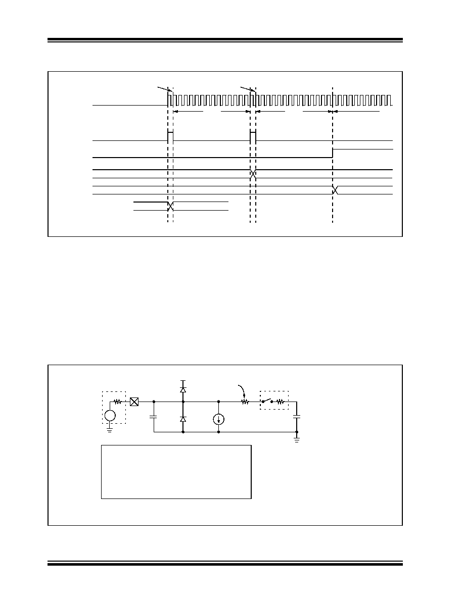
FIGURE 19-4:
12-BIT A/D CONVERTER ANALOG INPUT MODEL
TCONV
= 14 TAD
TSAMP
= 1 TAD
TSAMP
= 1 TAD
ADCLK
SAMP
DONE
ADCBUF0
ADCBUF1
Instruction Execution BSET ADCON1, ASAM
TCONV
= 14 TAD
CPIN
VA
Rs
ANx
VT = 0.6V
ILEAKAGE
RIC
250
Sampling
Switch
RSS
CHOLD
= DAC capacitance
VSS
VDD
= 18 pF
500 nA
Legend: CPIN
VT
ILEAKAGE
RIC
RSS
CHOLD
= Input Capacitance
= Threshold Voltage
= Leakage Current at the pin due to
= Interconnect Resistance
= Sampling Switch Resistance
= Sample/Hold Capacitance (from DAC)
various junctions
Note: CPIN value depends on device package and is not tested. Effect of CPIN negligible if Rs
2.5 k.
RSS
3 k
发布紧急采购,3分钟左右您将得到回复。
相关PDF资料
DSPIC30F5013-30I/PT
IC DSPIC MCU/DSP 66K 80TQFP
DSPIC30F5015-30I/PT
IC DSPIC MCU/DSP 66K 64TQFP
DSPIC30F6010-20E/PF
IC DSPIC MCU/DSP 144K 80TQFP
DSPIC30F6010A-30I/PF
IC DSPIC MCU/DSP 144K 80TQFP
DSPIC30F6013A-30I/PF
IC DSPIC MCU/DSP 132K 80TQFP
DSPIC30F6014-30I/PF
IC DSPIC MCU/DSP 144K 80TQFP
DSPIC33EP512MU814-I/PL
IC DSC 16BIT 512KB 144LQFP
DSPIC33EP64MC504-E/TL
IC DSC 16BIT 64KB FLASH 44-VTLA
相关代理商/技术参数
DSPIC30F4013-30I/P
功能描述:数字信号处理器和控制器 - DSP, DSC General Purpose RoHS:否 制造商:Microchip Technology 核心:dsPIC 数据总线宽度:16 bit 程序存储器大小:16 KB 数据 RAM 大小:2 KB 最大时钟频率:40 MHz 可编程输入/输出端数量:35 定时器数量:3 设备每秒兆指令数:50 MIPs 工作电源电压:3.3 V 最大工作温度:+ 85 C 封装 / 箱体:TQFP-44 安装风格:SMD/SMT
DSPIC30F4013-30I/P
制造商:Microchip Technology Inc 功能描述:16BIT MCU-DSP 30MHZ 30F4013 DIP40
DSPIC30F4013-30I/PT
功能描述:数字信号处理器和控制器 - DSP, DSC General Purpose RoHS:否 制造商:Microchip Technology 核心:dsPIC 数据总线宽度:16 bit 程序存储器大小:16 KB 数据 RAM 大小:2 KB 最大时钟频率:40 MHz 可编程输入/输出端数量:35 定时器数量:3 设备每秒兆指令数:50 MIPs 工作电源电压:3.3 V 最大工作温度:+ 85 C 封装 / 箱体:TQFP-44 安装风格:SMD/SMT
DSPIC30F4013-30I/PT
制造商:Microchip Technology Inc 功能描述:DIGITAL SIGNAL CONTROLLER 16 BIT ((NW))
dsPIC30F4013T-20E/ML
功能描述:数字信号处理器和控制器 - DSP, DSC 44LD 20MIPS 48 KB RoHS:否 制造商:Microchip Technology 核心:dsPIC 数据总线宽度:16 bit 程序存储器大小:16 KB 数据 RAM 大小:2 KB 最大时钟频率:40 MHz 可编程输入/输出端数量:35 定时器数量:3 设备每秒兆指令数:50 MIPs 工作电源电压:3.3 V 最大工作温度:+ 85 C 封装 / 箱体:TQFP-44 安装风格:SMD/SMT
dsPIC30F4013T-20E/PT
功能描述:数字信号处理器和控制器 - DSP, DSC 20MIPS 48 KB RoHS:否 制造商:Microchip Technology 核心:dsPIC 数据总线宽度:16 bit 程序存储器大小:16 KB 数据 RAM 大小:2 KB 最大时钟频率:40 MHz 可编程输入/输出端数量:35 定时器数量:3 设备每秒兆指令数:50 MIPs 工作电源电压:3.3 V 最大工作温度:+ 85 C 封装 / 箱体:TQFP-44 安装风格:SMD/SMT
DSPIC30F4013T-20I/ML
功能描述:IC DSPIC MCU/DSP 48K 44QFN RoHS:否 类别:集成电路 (IC) >> 嵌入式 - 微控制器, 系列:dsPIC™ 30F 产品培训模块:XLP Deep Sleep Mode
8-bit PIC® Microcontroller Portfolio 标准包装:22 系列:PIC® XLP™ 18F 核心处理器:PIC 芯体尺寸:8-位 速度:48MHz 连通性:I²C,SPI,UART/USART,USB 外围设备:欠压检测/复位,POR,PWM,WDT 输入/输出数:14 程序存储器容量:8KB(4K x 16) 程序存储器类型:闪存 EEPROM 大小:256 x 8 RAM 容量:512 x 8 电压 - 电源 (Vcc/Vdd):1.8 V ~ 5.5 V 数据转换器:A/D 11x10b 振荡器型:内部 工作温度:-40°C ~ 85°C 封装/外壳:20-DIP(0.300",7.62mm) 包装:管件 产品目录页面:642 (CN2011-ZH PDF) 配用:DV164126-ND - KIT DEVELOPMENT USB W/PICKIT 2DM164127-ND - KIT DEVELOPMENT USB 18F14/13K50AC164112-ND - VOLTAGE LIMITER MPLAB ICD2 VPP
DSPIC30F4013T-20I/PT
功能描述:IC DSPIC MCU/DSP 48K 44TQFP RoHS:否 类别:集成电路 (IC) >> 嵌入式 - 微控制器, 系列:dsPIC™ 30F 产品培训模块:XLP Deep Sleep Mode
8-bit PIC® Microcontroller Portfolio 标准包装:22 系列:PIC® XLP™ 18F 核心处理器:PIC 芯体尺寸:8-位 速度:48MHz 连通性:I²C,SPI,UART/USART,USB 外围设备:欠压检测/复位,POR,PWM,WDT 输入/输出数:14 程序存储器容量:8KB(4K x 16) 程序存储器类型:闪存 EEPROM 大小:256 x 8 RAM 容量:512 x 8 电压 - 电源 (Vcc/Vdd):1.8 V ~ 5.5 V 数据转换器:A/D 11x10b 振荡器型:内部 工作温度:-40°C ~ 85°C 封装/外壳:20-DIP(0.300",7.62mm) 包装:管件 产品目录页面:642 (CN2011-ZH PDF) 配用:DV164126-ND - KIT DEVELOPMENT USB W/PICKIT 2DM164127-ND - KIT DEVELOPMENT USB 18F14/13K50AC164112-ND - VOLTAGE LIMITER MPLAB ICD2 VPP